


STMicroelectronics STDRIVEG610 Half-Bridge Gate Drivers
STMicroelectronics STDRIVEG610 Half-Bridge Gate Drivers are high-performance devices designed for driving N-channel MOSFETs or IGBTs in a variety of power conversion applications. The STMicroelectronics STDRIVEG610 features a single input control and bootstrap operation, enabling efficient high-side and low-side switching with minimal external components. The devices support up to 600V on the high-side driver and include under-voltage lockout (UVLO) protection on both the low-side and high-side to ensure safe operation. With a typical propagation delay of 50ns and matched delay times, the STDRIVEG610 ICs are well-suited for high-frequency switching applications such as motor control, power supplies, and inverters. The compact design, robust protection features, and wide operating voltage range make the STDRIVEG610 Half-Bridge Gate Drivers a reliable choice for designers seeking efficient and compact gate driver solutions.
Features
- Up to 600V high voltage rail
- ±200V/ns dV/dt transient immunity
- Driver with a separated sink and source path for optimal driving
- 2.4A and 1.2Ω sink
- 1.0A and 3.7Ω source
- High-side and low-side linear regulators for 6V gate driving voltage
- 300ns, ultra-fast high-side startup time
- 45ns propagation delay, 15ns minimum output pulse
- High (>1MHz) switching frequency
- Embedded 600V bootstrap diode
- Full support of GaN hard-switching operation
- UVLO function on VCC, VBO, and VLS
- Separated logic inputs and shutdown pin
- Fault pin for overtemperature and UVLO reporting
- Stand-by function for low consumption mode
- Separated PGND for Kelvin source driving and current shunt compatibility
- 3.3V to 20V compatible inputs with hysteresis and pull-down
Applications
- DC/DC and resonant converters (LLC, active clamp flyback, totem pole, ...)
- PFC and synchronous rectifier topologies
- Battery chargers and adapters
- AC/DC converters
Specifications
- 9.2V to 18V logic supply voltage range
- ±3V low-side driver ground
- 7.5V to 20V VBOOT-OUT pin voltage range
- -10.8VDC to 520VDC output voltage range
- 600V maximum transient output voltage
- 0V to 20V logic inputs voltage range
- 47nF to 220nF driver supply voltage bypass capacitance range
- 3300nF maximum high-side driver linear regulator input capacitance
- 50ns minimum duration of input pulse
- 2MHz maximum switching frequency
- Thermal resistance
- 85°C/W junction-to-ambient when mounted on a 2s2p (4-layer) FR4 board according to JESD51-7 without PCB thermal vias
- 110°C/W junction-to-ambient when mounted on a 1s0p (1-layer) FR4 board according to JESD51-3
- ESD ratings
- 2kV Human Body Model per ANSI/ESDA/JEDEC JS-001-2017
- 1kV Charged Device Model per ANSI/ESDA/JEDEC JS-002-2018
- -40°C to +125°C junction temperature range
- 4mm x 5mm x 1mm QFN package
Typical Application Schematic

Block Diagram

Development Tool
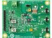
STMicroelectronics EVLSTDRIVEG610Q Evaluation Board
Based on the STDRIVEG610 high-speed, half-bridge gate driver that is optimized to drive GaN HEMTs.
Videos
Related Drivers
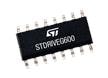
STMicroelectronics STDRIVEG600/210/211 Half-Bridge Gate Drivers
Single-chip half-bridge gate driver for Enhancement mode GaN FETs or N-channel power MOSFETs.
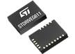
STMicroelectronics STDRIVEG611 Half-Bridge Gate Driver
A high-voltage half-bridge gate driver for N-channel Enhancement Mode GaN.
Published: 2025-06-19
| Updated: 2025-08-07