


Texas Instruments LMK05318B Network Synchronizer Clock
Texas Instruments LMK05318B Network Synchronizer Clock provides jitter cleaning, clock generation, advanced clock monitoring, and superior hitless switching performance. These are all to meet the stringent timing requirements of communications infrastructure and industrial applications. The device's ultra-low jitter and high power supply noise rejection (PSNR) can reduce bit error rates (BER) in high-speed serial links. The Texas Instruments LMK05318B can generate output clocks with 50fs RMS jitter using TI's proprietary Bulk Acoustic Wave (BAW) VCO technology, independent of the jitter and frequency of the XO and reference inputs.
The DPLL supports programmable loop bandwidth for jitter and wander attenuation, while the two APLLs support fractional frequency translation for flexible clock generation. The synchronization options supported on the DPLL include hitless switching with phase cancellation, digital holdover, and DCO mode with less than 0.001ppb (part per billion) frequency step size for precision clock steering (IEEE 1588 PTP slave). The DPLL can phase-lock to a 1PPS (pulse-per-second) reference input and support optional zero-delay mode on one output to achieve deterministic input-to-output phase alignment with programmable offset. The advanced reference input monitoring block ensures robust clock fault detection and helps to minimize output clock disturbance when a loss of reference (LOR) occurs. The LMK05318B-Q1 devices are AEC-Q100 qualified for automotive applications
The LMK05318B can use a commonly available low-frequency TCXO or OCXO to set the free-run or holdover output frequency stability per synchronization standards. Otherwise, the device can use a standard XO when free-run or holdover frequency stability and wander are not critical. The device is fully programmable through an I2C or SPI interface and supports custom frequency configuration on power-up with the internal EEPROM or ROM. The EEPROM is factory pre-programmed and can be programmed in-system if needed.
Features
- One Digital Phase-Locked Loop (DPLL) with
- ±50ps phase transient hitless switching
- Programmable loop bandwidth with fast lock
- Standards-compliant synchronization and holdover using a low-cost TCXO/OCXO
- Two Analog Phase-Locked Loops (APLLs) with industry-leading jitter performance
- 50fs RMS jitter at 312.5MHz (APLL1)
- 130fs RMS jitter at 155.52MHz (APLL2)
- Two reference clock inputs
- Priority-based input selection
- Digital holdover on the loss of reference
- Eight clock outputs with programmable drivers
- Up to six different output frequencies
- AC-LVDS, AC-CML, AC-LVPECL, HCSL, and 1.8V LVCMOS output formats
- EEPROM / ROM for custom clocks on power-up
- Flexible configuration options
- 1Hz (1PPS) to 800MHz on input and output
- 10 to 100MHz XO/TCXO/OCXO input
- < 0.001ppb/step for precise clock steering (IEEE 1588 PTP slave) DCO Mode
- Advanced clock monitoring and status
- I2C or SPI interface
- PSNR: –83dBc (50mVpp noise on 3.3V supply)
- 3.3V supply with 1.8V, 2.5V, or 3.3V outputs
- –40°C to +85°C industrial temperature range
- LMK05318B-Q1 is AEC-Q100 qualified
- for automotive applications
- -40°C to 105°C temperature grade 2
Applications
- SyncE (G.8262), SONET/SDH (Stratum 3/3E, G.813, GR-1244, GR-253), IEEE 1588 PTP slave clock, or optical transport network (G.709)
- 400G line cards, fabric cards for ethernet switches and routers
- Wireless Base Station (BTS), wireless backhaul
- Test and measurement, medical imaging
- Jitter cleaning, wander attenuation, and reference clock generation for 56G/112G PAM-4 PHYs, ASICs, FPGAs, SoCs, and processors
Functional Block Diagram

Related Development Tool
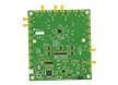
Texas Instruments LMK05318BEVM Clock Evaluation Module (EVM)
Designed for the evaluation of the LMK05318B, a network synchronizer clock device.