


Texas Instruments SN74LVC125A/SN74LVC125A-Q1 Quad Bus Buffer Gate
Texas Instruments SN74LVC125A/SN74LVC125A-Q1 Quadruple Bus Buffer Gate has independent line drivers with 3-state outputs. Each output is disabled when the associated output-enable (OE) input is high. The OE should be tied to VCC through a pullup resistor to ensure the high-impedance state during power up or down. The current-sinking capability of the driver determines the minimum value of the resistor. Each of the inputs can be driven from either 3.3V or 5V devices. This feature allows the use of this device as a translator in a mixed 3.3V/5V system environment. This quadruple bus buffer gate is designed for 1.65V to 3.6V VCC operation. The Texas Instruments SN74LVC125A-Q1 devices are AEC-Q100 qualified for automotive applications and the SN74LVC125A-EP devices have gold bond wires, a temperature range of –55 to +105°C, and an SnPb lead finish.
Features
- 3-state outputs
- Separate OE for all 4 buffers
- Operates from 1.65V to 3.6V
- Specified from -40°C to 125°C
- Inputs accept voltages to 5.5V
- Max tpd of 4.8ns at 3.3V
- Typical VOLP (output ground bounce) <0.8V at VCC = 3.3V, TA = 25°C
- Typical VOHV (output VOH undershoot) >2V at VCC = 3.3V, TA = 25°C
- Latch-up performance exceeds 250mA per JESD 17
Functional Block Diagram

Related Buffer Gates

Texas Instruments SN74LVC126A/SN74LVC126A-Q1 Buffer Gates
Feature independent line drivers with 3-state outputs and are ideal for AV receivers.
Related Development Tools
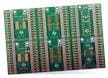
Texas Instruments 14-24-LOGIC-EVM Logic Evaluation Module (EVM)
Generic evaluation module developed to support any TI logic leaded device in a 14 to 24 pin count.
Texas Instruments 14-24-NL-LOGIC-EVM Logic Evaluation Module (EVM)
Supports any logic or translation device in a BQA, BQB, RGY (14-24 pin), RSV, RJW, or RHL package.
Published: 2024-04-03
| Updated: 2025-08-01